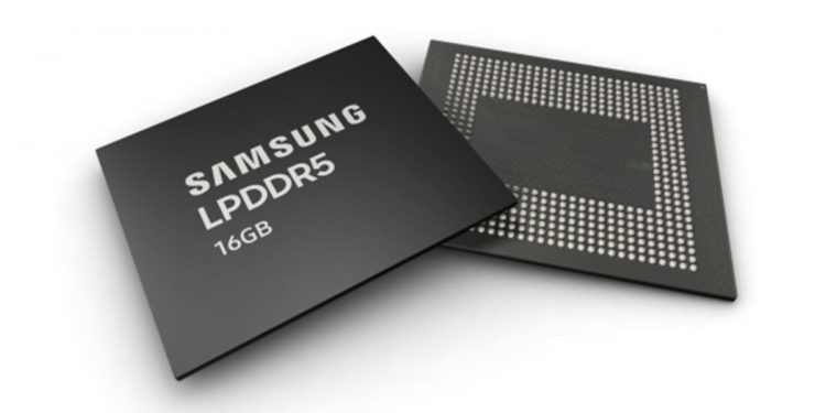
Samsung Electronics said on Sunday that it began mass production of the first 16-gigabyte (Gb) LPDDR5 mobile DRAM chip at its second production line in Pyeongtaek, South Korea.
Samsung’s latest mobile DRAM chip, built on its third-generation 10nm-class (1z), utilizes extreme ultraviolet (EUV) technology in production. It features the utmost mobile memory performance and largest storage capacity allowing more users to maximize the benefits of 5G and AI properties of next-generation smartphones.
Jung-bae Lee, executive VP of DRAM Product & Technology at Samsung Electronics, stated that the new chip conquered developmental difficulties and elevated the industry to a new beginning. Samsung would expand its premium DRAM assembly to meet demands and lead the memory chip industry.
Constructed in 2018, Pyeongtaek Line 2 spans over 128,900 square meters, making it the most extensive semiconductor production line globally.
Samsung intends to construct a second fabrication plant in Pyeongtaek and plans to spend 30 trillion won ($25 billion). The second fabrication plant would also include a foundry and NAND flash manufacturing sites. These facilities would completely operate by midyear of 2021.
Faster-Than-Ever Transfer Speed
The new LPDDR5 chip works 16 percent faster than the 12Gb LPDDR5 currently used in most mobile devices. The chip could transfer data at a rate of 6,400 megabits per second. It could transfer 51.2 GB data in one second when made into a 16GB package.
The chip displays a 30 percent thinner casing than its predecessor, enabling 5G and allows smartphone devices access to more functional features. The 16GB LPDDR5 could also build a 16GB package using only eight chips.
Samsung intends to reinforce its leadership in the market by providing the first 1z-based 16GB LPDDR5 to smartphone makers worldwide. The company plans to develop its LPDDR5 into automotive systems with temperature range solutions for safety and reliability in extreme conditions.


